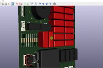
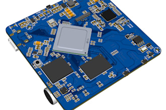
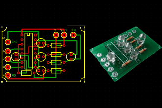
I will design rf pcb antenna layout and high speed pcb with impedance control
About this Gig
Need a professional RF PCB engineer for your wireless, IoT, wearable, or high-speed electronics project? I will create a clean, reliable, and manufacturing-ready board layout with proper RF routing and impedance control.
My services include:
- RF PCB layout and routing
- Antenna PCB layout
- High-speed circuit boards
- Controlled impedance routing
- Differential pair routing
- WiFi, Bluetooth/BLE, LoRa and GSM boards
- IoT and wearable electronics
- Multilayer PCB development
- DRC, Gerber, BOM and Pick & Place files
I focus on proper component placement, grounding, signal integrity, RF performance, impedance matching, compact board size, and manufacturability.
I work with KiCad, Altium Designer, and other professional PCB tools.
Before ordering, please send your schematic, board dimensions, layer count, stackup, component files, and project requirements. This allows me to understand your requirements and recommend the right package.
Lets turn your schematic into a professional RF or high-speed PCB ready for manufacturing.
Other Electronics Engineering Services I Offer
FAQ
What information do you need to start?
Please provide your schematic, PCB dimensions, component/footprint files, required layer count, stackup information, and any RF or impedance requirements you have
Can you handle RF and antenna PCB layouts?
Yes. I can work on RF routing, antenna placement, impedance-controlled traces, grounding, matching networks, and wireless PCB layouts for applications such as WiFi, Bluetooth/BLE, LoRa, and GSM.
Can you work with KiCad or Altium?
Yes. I can work with KiCad and Altium Designer and provide the appropriate source and manufacturing files based on your project requirements.
Do you provide manufacturing files?
Yes. Depending on the package, I can provide Gerber files, drill files, BOM, Pick & Place files, and other manufacturing outputs required by your PCB manufacture
Can you work with multilayer and high-speed PCBs?
Yes. I can handle 2-layer, 4-layer, and multilayer boards, including high-speed routing, differential pairs, controlled impedance, signal integrity considerations, and compact PCB layouts.