Browse categories
Explore
Fiverr Pro
English
$
USD
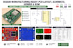
Are you looking for a clean, accurate and manufacturing ready PCB for your project? You are in the right place. I will de sig n a professional PCB layout and circuit schematic with optimized routing and production ready files for your electronic project.
If you need a simple board, custom hardware solution, prototype design, IoT board or multilayer PCB, I can help turn your idea in to a reliable de sig n ready for manufacturing.
What you will receive:
I can work with KiCad, Altium Designer, EasyEDA and other PCB tools.
I focus on clean routing, component placement, design accuracy and delivering files that are ready for prototype and production use.
Kindly contact me before placing an order so I can understand your project requirements and provide the best solution.

File format:
Gerber
•
STEP
•
BRD
•
SCH
•
Software:
Altium Designer
•
EasyEDA
•
KiCad
•
LTspice
•
AutoCAD
•
PSpice
Interface:
HDMI
•
I2S
•
UART
•
SPI
•
SDIO
•
Wi-Fi
•
Ethernet
