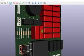
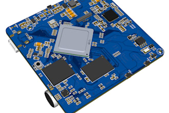
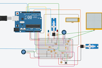
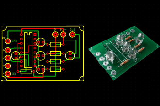
I will do rf radio pcb design multilayer pcb layout rigid flex pcb gerber for prototype
eLearning LMS Setup SCORM 3D CAD Modeling and PCB Electronics Development Expert
About this Gig
Struggling to get an RF radio PCB design that actually works the first time? Poor PCB layout de-sign, noisy signals, failed prototypes, EMI issues, costly PCB revisions, and manufacturing errors can delay your product and increase expenses. Whether you need RF radio PCB de-sign, multilayer PCB layout, rigid flex PCB, PCB, PCB layout design, Gerber files, prototype PCB, high-speed PCB, or manufacturing-ready PCB, this gig is built to deliver reliable, production-ready results. Every PCB and PCB layout design is optimized for performance, manufacturability, and accurate fabrication.
I provide complete PCB de-sign and PCB layout design solutions for RF, multilayer, and rigid flex projects, ensuring clean routing, optimized signal integrity, accurate component placement, and fabrication-ready Gerber files. Every project is reviewed for quality before delivery, with revisions until the agreed requirements are met.
Services:
- RF Radio PCB
- PCB Layout De-sign
- Multilayer PCB
- Rigid Flex PCB
- Schematic De-sign
- Gerber Files
- BOM Creation
- DFM Review
- Prototype Support
Niches:
- RF PCB
- High-Speed PCB
- IoT PCB
- Embedded PCB
- Industrial PCB
- Automotive PCB
- Audio PCB
- Wireless PCB
Message Me Today!
FAQ
Do you design RF PCB for wireless products?
Yes, I design RF PCB with proper impedance control and antenna placement for reliable wireless performance.
Can you fix a PCB design that already failed manufacturing or testing?
Yes. Send me your existing Gerber files or schematic, and I'll audit it for the root cause, impedance mismatch, footprint errors, or DFM violations, then correct it before you reorder from the fab house.
What software do you use for RF PCB design and multilayer layout?
I work in Altium Designer, KiCad, and EasyEDA. I'll match your preferred software or recommend the best fit for your project's complexity, especially for RF and rigid-flex boards.
How do you handle RF interference or signal loss issues in my design?
I apply controlled impedance routing, proper ground planes, and correct antenna placement to prevent the noise and signal degradation that cause most RF board failures.
Can rigid-flex PCBs handle repeated bending without cracking?
Yes, when designed correctly. I place components and routing away from flex zones and follow bend-radius guidelines so your board survives real-world flexing, not just prototype testing.
What if I only have an idea, not a finished schematic?
No problem. Share your concept, features, and constraints, and I'll build the schematic from scratch before moving into layout.
How many layers do I actually need for my project?
Tell me your board's function, size, and RF/wireless requirements, and I'll recommend 2, 4, 6+ layers based on what solves your specific noise, space, or performance needs, not a generic default.
Can you work with tight deadlines for urgent prototypes?
Yes, message me your timeline before ordering. I can prioritize rush projects to prevent costly production delays on your end.
Do you sign NDAs to protect my design?
Absolutely. I'll sign your NDA or mine before any files are shared, so your IP stays fully protected.