Browse categories
Explore
Fiverr Pro
English
$
USD
Custom PCB Design, Electronics Engineering and Simulation Expert
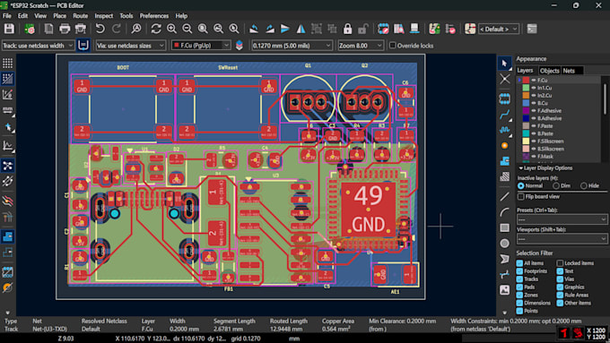
I specialize in reliable PCB design, schematic setup, and circuit simulation using KiCad and LTspice. Whether you need a simple breakout board, an IoT device, or a multi-layer layout, I will make sure your design is ready for the factory.
What You Will Get:
Why Choose Me?
I design your board following factory standards (DFM/DFA). This means your files will work perfectly with manufacturers like JLCPCB or PCBWay without any errors or rejections.
Please message me before placing an order. Let's talk about your project first so we can pick the perfect package for you!


What software do you use for PCB design?
I use KiCad for all schematic capture and PCB layout design. For circuit simulation and testing, I use LTspice to make sure everything works perfectly before manufacturing.
What files will I receive at delivery?
You will get a complete manufacturing package. This includes production-ready Gerber files, NC Drill files, a BOM (Bill of Materials), a 3D model of your board, and PDF schematic sheets.
Can you design my board for JLCPCB or PCBWay?
Yes! I design all circuit boards following strict DFM (Design for Manufacturing) standards. Your files will be fully optimized to pass factory checks smoothly on major fabrication houses without any rejections.