Browse categories
Explore
Fiverr Pro
English
$
USD
PCB Design Engineer Circuit Schematic and Electronics Design Specialist
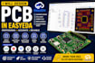
Looking for a professional EasyEDA PCB designer?
I will create high-quality PCB layouts and circuit schematics using EasyEDA for your electronics project.
Services Include:
Perfect For:
Why Choose Me?
Contact me before ordering to discuss your project requirements.

Specialization:
Circuit design
•
Schematics
•
Layout
File format:
STEP
•
3DS
Software:
Cadence OrCAD
•
EasyEDA
•
AutoCAD
What files will I receive?
EasyEDA source files, Gerber files, BOM, PDF schematics, and PCB layouts.
Can you design multi-layer PCBs?
Yes, I can design single-layer, double-layer, and multi-layer boards.
Can you redesign an existing PCB?
Yes, I can modify, improve, or redesign existing PCB layouts.
Are the files ready for manufacturing?
Yes, all required manufacturing files will be provided.


