Browse categories
English
$
USD
Connect to your AI
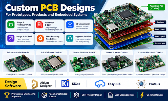
Looking for a professional PCB for your electronic product or prototype?
I provide PCB and electronic engineering services, from schematic development to PCB layout and manufacturing-ready files.
My Services:
PCB Layout (Single & Multilayer)
Schematic & Circuit Development
Bill of Materials (BOM) Creation
Gerber & Drill File Generation
Component Placement and Routing
Design Rule Checks (DRC)
Microcontroller & Embedded System Boards
Sensor Interfaces and Custom Electronic Circuits
3D PCB Visualization
Deliverables:
Depending on your package, you can receive PCB source files, schematics, BOM, Gerber files, drill files, and documentation.
Software: Altium Designer, KiCad, EasyEDA, and Proteus.
I focus on clean layouts, practical component placement, accuracy, and organized project files.
Before ordering: Please share your circuit diagram, project requirements, board dimensions, component list, and preferred software. Contact me for complex or multilayer designs so we can agree on the scope and price.
Let's turn your electronic idea into a professional PCB design!
What do you need to start my PCB design?
To begin your PCB design, I need your project requirements such as block diagram, reference design, component list (if available), board size, number of layers, and application details. If you don’t have everything, I can also help from the concept and schematic design stage.
Do you provide schematic design and BOM?
Yes. I provide complete schematic design, PCB layout, and BOM creation. You will receive a fully documented manufacturing-ready PCB design including Gerber files and component sourcing support.
Can you design multilayer and high-speed PCBs?
Absolutely. I specialize in multilayer PCB design (1–8 layers), high-speed PCB routing, power integrity, and signal integrity following DFM/DFA standards for reliable fabricatio
What files will I receive after completion?
You will receive Gerber files, drill files, pick-and-place files, schematic, BOM, and a fabrication-ready PCB package. A 3D PCB preview can also be provided if required.
Is the PCB design ready for manufacturing?
Yes. All PCB designs are optimized for manufacturability and assembly, following DFM/DFA guidelines, ensuring smooth PCB fabrication and assembly.
Which PCB design tools do you use?
I use Altium Designer, EasyEDA, KiCad, and Proteus depending on project requirements and client preference.
Do you provide revisions and support?
Yes. I offer revisions, testing support, and long-term assistance for future updates, revisions, and production scaling.