Browse categories
Explore
Fiverr Pro
English
$
USD
Expert PCB Layout, Schematic and Gerber Design
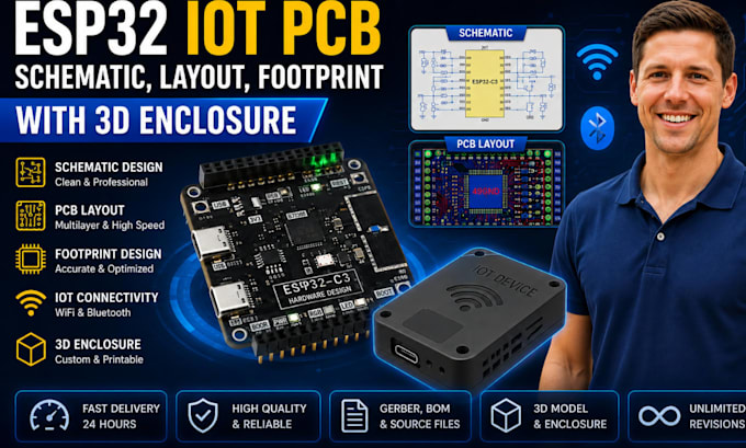
Need a reliable ESP32 IoT PCB with a professional schematic, PCB layout, custom footprints, and 3D enclosure?
I can turn your concept into a clean, functional, and fabrication-ready hardware design.
I will design you ESP32/IoT PCB, including schematic capture, component placement, routing, custom footprints, BOM, Gerber files, 3D PCB modeling, and a custom 3D-printable enclosure.
What I offer:
Tools I use:
Whether you need a compact IoT device, sensor board, ESP32 controller, or complete enclosed product, Ill deliver a professional design ready for manufacturing and prototyping.
Send your requirements, schematic, datasheets, or project concept to get started.
Specialization:
Circuit design
•
Schematics
•
Layout
•
Footprint
•
Gerber
File format:
Gerber
•
STEP
•
VRML
•
3DS
•
Software:
CircuitMaker
What PCB software do you use?
I use KiCad, Altium Designer, and EasyEDA for schematic and PCB design.
Can you design a custom ESP32 IoT PCB?
Yes. I can design custom ESP32 boards with sensors, modules, connectors, power circuits, and communication interfaces.
Do you create custom footprints?
Yes, I can create and verify custom component footprints based on datasheets.
Can you design a 3D enclosure?
Yes. I can create a custom 3D-printable enclosure that fits your PCB and components.
Can you work from an idea instead of a schematic?
Yes. Send your requirements, block diagram, reference design, or project concept, and I can help develop the PCB design.
Can you design multilayer PCBs?
Yes. I can design 2–6 layer PCBs, depending on the project requirements.