Browse categories
English
$
USD
Connect to your AI
Pcb designer
HELLO AND WELCOME!
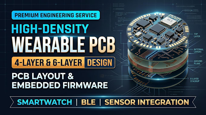
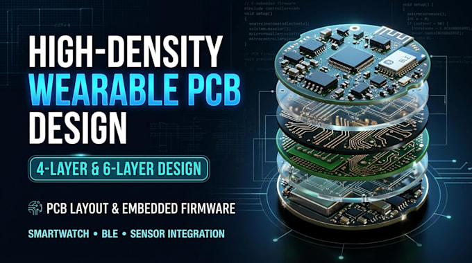
Developing high-density wearable electronics requires more than compact component placement; it demands precise multilayer PCB engineering, signal integrity control, power optimization, and efficient embedded processing within extremely limited physical dimensions.
What I Will Provide;
Why Choose Me?
Ready to bring your wearable electronics concept to life? message now and Let's develop a compact, high-performance PCB with optimized hardware and intelligent embedded firmware!!!!.



Can you design both 4-layer and 6-layer wearable PCBs?
Yes, I can develop 4-layer and 6-layer PCB layouts based on your component density, routing requirements, and electrical specifications.
What wearable devices can you work on?
I can work on smartwatches, fitness trackers, smart bands, health-monitoring wearables, and custom miniature electronics.
Can you integrate wireless connectivity?
Yes, I can integrate BLE, Wi-Fi, NFC, and other wireless communication modules where required.
Do you provide embedded firmware?
Yes, I develop embedded C/C++ firmware for microcontrollers, sensors, wireless communication, and power management.
Can you design battery-powered wearable electronics?
Yes, I can implement battery charging, voltage regulation, power monitoring, and low-power operating architectures.
Which PCB design software do you use?
I can work with professional PCB design tools such as Altium Designer, KiCad, and other compatible EDA platforms.
Will you provide manufacturing files?
Yes, deliverables can include Gerber files, drill files, BOM, pick-and-place data, and fabrication-ready documentation.
Can you work with an existing PCB design?
Yes, I can review, optimize, modify, and improve existing schematics and PCB layouts.