Browse categories
Explore
Fiverr Pro
English
$
USD
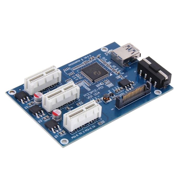
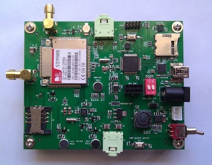
Expert PCB Designer, Multilayer Layouts and IoT Hardware
Are PCB errors, poor routing, or failed manufacturing costing you time and money? I design production-ready PCB layouts and schematics that are optimized for performance, reliability, and smooth fabrication.
I will turn your idea, sketch, or existing circuit into a professional PCB design using industry-standard tools, ensuring clean routing, proper component placement, and full DFM readiness.
What you'll get:
Tools & Software:
Advanced Capabilities:
Why choose me:
Send me your requirements before ordering, and lets bring your project to life.


What do I need to provide to get started?
The best starting point is a clear circuit diagram or a hand-drawn sketch of your idea. If you also have a list of specific components you want to use (a Bill of Materials) and the required dimensions of the board, that helps me jump straight into the design process.
Can you help if I only have a rough idea and no schematic?
I can help you develop the schematic from scratch based on your project requirements. Just send me a message with what you’re trying to achieve, and we can map out the components and connections together before I move to the PCB layout.
Will my board be ready for immediate manufacturing?
Yes, that is the goal. I provide a complete "Production Package" which includes Gerber files, Excellon drill files, and the Bill of Materials (BOM). These are the standard files that any fabrication house (like JLCPCB, PCBWay, or OshPark) requires to print your boards.
What if the manufacturer finds an issue with the design?
I design with DFM (Design for Manufacturing) principles to prevent this, but if a fabricator raises a technical query or a "Design Rule Check" (DRC) error, I will provide the necessary support and file updates to ensure the board gets made correctly.
Do you handle high-speed or complex RF designs?
Yes, I have experience managing signal integrity, impedance matching, and thermal optimization for more sensitive projects. Whether it’s a simple power breakout or a complex multilayer board with high-speed data lines, I ensure the routing is clean and interference-free.
Which software will you use for my project?
I’m flexible! I work across all major industry tools including Altium Designer, KiCad, Eagle, and EasyEDA. If you have a specific preference, or if you need the source files to match your own software for future edits, just let me know.
Can I get a 3D model of the finished board?
Yes, I include a 3D STEP file of the completed PCB (optional). This is incredibly useful if you are designing an enclosure or housing, as it allows you to check for component clearances and fitment in your CAD software.