Browse categories
Explore
Fiverr Pro
English
$
USD
Powering Innovation with MATLAB and Circuit Design
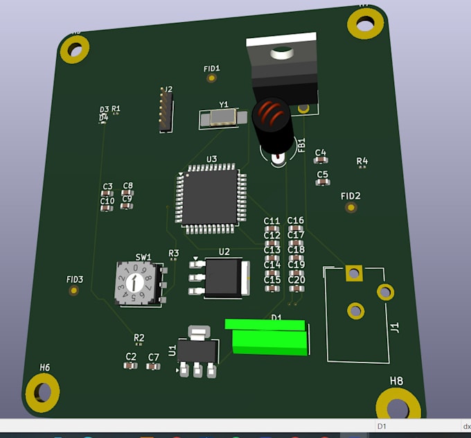
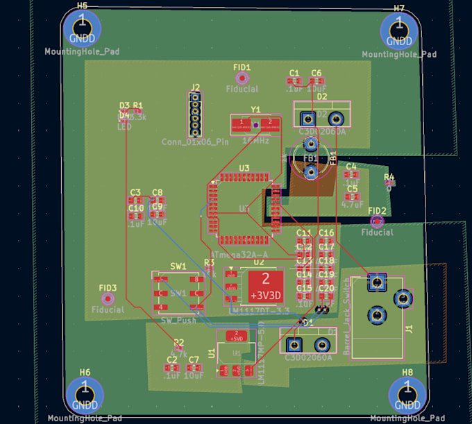
I will design high-quality PCB layouts and schematics tailored to your requirements. With expertise in circuit design, signal integrity, and manufacturability, I ensure your boards are optimized for performance and ready for fabrication.
Services I provide:
Tools I use:
Why choose me?
Deliverables:


File format:
Gerber
•
STEP
•
SCH
•
3DS
•
Software:
EasyEDA
•
KiCad
•
Matlab
•
Proteus
•
Simulink
•
AutoCAD
Interface:
HDMI
•
MIPI DSI/CSI
•
USB
•
SPI
•
I2C
•
LTE
Which PCB design software do you use?
I mainly use KiCad . I can also work with EasyEDA if you prefer.
Will you provide manufacturing files?
Yes, I will provide Gerber files, drill files, BOM, and pick-and-place files ready for fabrication at PCB manufacturers like JLCPCB, PCBWay, etc.
Can you design multi-layer PCBs?
Yes, I can design single-layer, double-layer, and multi-layer (up to 8 layers, depending on complexity).