Browse categories
Explore
Fiverr Pro
English
$
USD
3D CAD and Product Design, Expert Precision Models Ready for Production
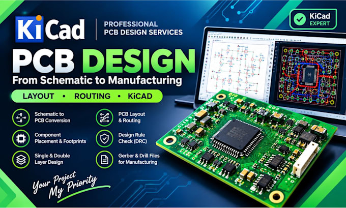
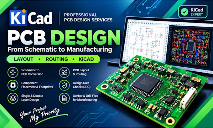
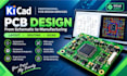
Need a professional PCB layout and routing service for your electronic project? I use KiCad to transform your circuit schematic into an organized board layout based on your components, dimensions, and manufacturing requirements.
What I Offer:
Why Choose Me?
I focus on circuit requirements, component footprints, board dimensions, and manufacturer specifications to produce a practical layout suited to your project. Each task is handled according to the agreed requirements and scope.
What You'll Get:
Depending on your package, deliverables may include editable KiCad project files, PCB layout files, Gerber files, drill files, and a 3D board preview. DRC results will also be reviewed within the agreed scope.
Let's Build Your PCB
Before ordering, send your circuit schematic, component list, board dimensions, preferred layer count, and manufacturing requirements. I'll review your project and confirm the appropriate scope and deliverables before work begins.
Specialization:
Circuit design
•
Schematics
•
Layout
•
Footprint
File format:
Gerber
•
SCH
•
•
Pcbdoc
Software:
EasyEDA
Interface:
I2S
•
I2C
•
SDIO
•
BLE
What do you need to start?
My schematic, component list, board dimensions, and design requirements.
Can you convert my schematic to a PCB?
Yes, if the schematic and project requirements are suitable.
What files will I receive?
KiCad files, Gerber files, drill files, and 3D preview, depending on your package.
Are the files ready for manufacturing?
I prepare manufacturing files and perform design rule checks within the agreed scope.
Can you handle my project?
Share your schematic and requirements so I can confirm the scope before ordering.