Browse categories
Explore
Fiverr Pro
English
$
USD
Product Design and PCB Engineer Precise Clean Production Ready
You have a working circuit on breadboardbut a poor PCB design leads to noise, ground bounce, trace errors and Gerber rejection, costing extra prototype cycles.
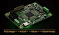
I design fabrication-ready PCBs with clean schematic, optimized layout and production files so your circuit works exactly as intended from first build.
I OFFER:
YOU GET:
WHY ME:
Message me with your schematic or idea to confirm layers, components and timeline before

Will my PCB layout be original or reused from another project?
Every schematic and PCB layout is designed from scratch for your specific circuit. No existing designs are modified or reused. Your project is treated as fully confidential and the files are yours exclusively on delivery.
How do you ensure the board will work after fabrication?
Every layout undergoes full DRC and ERC checks before delivery. Component footprints are verified against datasheets, power trace widths are calculated for current capacity, and Gerber files are cross-checked against manufacturer design rules. I also include a 3D PCB model for mechanical clearance
Can you deliver a PCB design urgently?
Yes. Message me before ordering with your component count and deadline. Simple 2-layer boards with a clear schematic can often be delivered in 1 to 2 days. Multilayer high-speed designs need more time for proper routing and signal integrity review.
What files will I receive at delivery?
Gerber and drill files, PDF schematic, BOM in CSV and source files in KiCad or Altium format. Premium orders also include pick and place CPL files and a 3D PCB STEP model.
What do I need to provide before you start?
Share your circuit concept or existing schematic, component list with datasheet links, microcontroller or module choice, layer count preference, board size constraints and preferred software format — KiCad, Altium or EasyEDA.
Can you help if I only have a rough circuit idea and no schematic?
Yes. Message me with your circuit goals, the problem you are solving and the components you want to use. I can guide you through schematic development before moving to the PCB layout.
