Browse categories
Explore
Fiverr Pro
English
$
USD
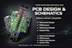
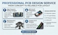
Professional PCB Design Schematics Layout, Gerber Files And Product Enclosure
Are you looking for a professional PCB designer who delivers fabrication-ready boards on time, first-time pass guaranteed?
I'm a certified Electronics & Hardware Engineer with hands-on expertise in PCB schematic deslgn, PCB layout deslgn, and signal integrity optimization using Altium Deslgner, KiCad, and EasyEDA. Whether you're a startup launching your first IoT product, an engineer needing a quick PCB redeslgn, or a hardware team that needs a complex multi-layer board I deslgn it right, and I deslgn it to manufacture.
Core services
PCB board types covered
Every design is reviewed for deslgn-for-manufacture (DFM) issues before delivery no costly respins. You get clean, structured files your contract manufacturer can use directly. I communicate clearly throughout the project so there are no surprises. Message me before ordering