Browse categories
Explore
Fiverr Pro
English
$
USD
PCB ENGINEER FOR ANY KIND OF WORK OR PROJECT
Welcome to my PCB De-sign Gig!
Are you looking for a professional PCB designer to turn your idea into a reliable, manufacturing-ready product? You've come to the right place.
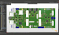
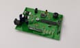
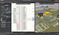
I specialize in PCB Design, PCB Layout, Circuit Schematic Des!gn, Gerber File Generation, BOM Creation, PCB Modification, Reverse Engineering, and complete electronic hardware development using Altium Designer.
What I can help you with:
My goal is to deliver accurate, efficient, and high-quality des!gns that meet your project requirements and manufacturing standards. Whether you need a simple PCB, a complex electronic system, or support for an ongoing project, I am available to help.
Client satisfaction, clear communication, and quality work are my top priorities.
Have questions or custom requirements? Send me a message anytime. I'm just a DM away and ready to help bring your electronics project to life.
What information do you need to start my PCB project?
Please provide your project requirements, circuit details, schematic (if available), dimensions, layer count, preferred components, and any special design specifications.
Which PCB design software do you use?
I primarily use Altium Designer to create professional schematics, PCB layouts, Gerber files, and manufacturing-ready designs.
Can you redesign or modify an existing PCB?
Yes. I can modify, improve, troubleshoot, optimize, or redesign existing PCB designs based on your requirements.
What files will I receive upon project completion?
Depending on the package, you will receive schematic files, PCB layout files, Gerber files, BOM (Bill of Materials), Pick-and-Place files, PDF documentation, and other manufacturing files.
Can you help with custom or complex electronics projects?
Absolutely. I am available for projects of all sizes, from simple PCB layouts to complex multilayer boards and complete electronic product development.


