Browse categories
Explore
Fiverr Pro
English
$
USD
PCB Design Embedded Systems Firmware Development Electronics Engineer
Hello and Welcome!
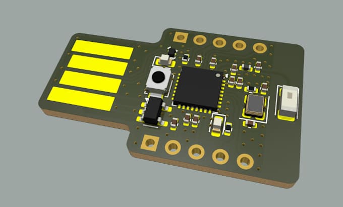
Need to fit powerful electronics into a tiny space? I specialize in ultra-compact PCB solutions.
I create high-density IoT PCBs with LTE, GPS, and RF antenna integration for wearable and space-constrained devices.
If you need a miniaturized solution that fits tight enclosures without compromising performance, I can help. I focus on compact layouts, efficient routing, and reliable hardware for advanced embedded systems.
What I Offer:
Why Choose Me:
Message me to discuss your project before ordering.

What do you need to start my PCB project?
I need your schematics, component list (if available), board size, and any specific requirements like RF, wearable constraints, or enclosure details.
Can you work with my existing schematic?
Yes, I can review, fix ERC errors, optimize footprints, and prepare it for a clean, manufacturable layout.
Do you design RF PCBs for LTE, GPS, or antennas?
Yes, I handle RF layout including LTE, GPS, antenna routing, grounding, and basic impedance considerations.
Can you design ultra-compact or wearable PCBs?
Absolutely. I specialize in miniaturization, high-density layouts, and compact designs for wearable and space-limited devices.
What files will I receive?
You’ll get Gerber files, BOM, pick-and-place (CPL), and source files (if requested), ready for JLCPCB or other manufacturers.
Which tools do you use?
I work with Altium, KiCad, EasyEDA, and other industry-standard tools depending on your project.
Can you help with component selection?
Yes, I can suggest components based on availability, cost, and performance for your application.
Do you support multi-layer and high-density boards?
Yes, I handle 2–6 layer boards with high-density routing and compact layouts.
Do you handle manufacturing support?
Yes, I provide JLCPCB-ready files and can guide you through ordering if needed.