Browse categories
Explore
Fiverr Pro
English
$
USD
PCB layout
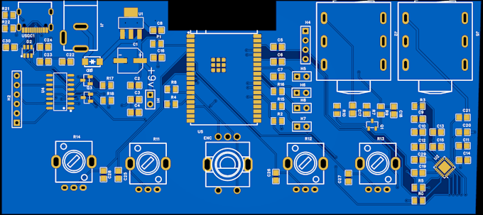
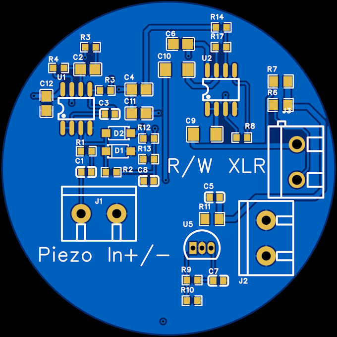
Need your schematic turned into a PCB you can actually order and build? I'm Ben, a trained electrician and electronics designer, and I lay out clean, manufacturable boards in KiCad or EasyEDA, ready for manufacture.
Because I build, solder and debug my own boards, I design with real assembly and testing in mind, not just a passing DRC.
What you get:
Specialties: analog and audio circuits (preamps, guitar pedals), microcontroller boards (Arduino, ESP32, Daisy Seed)
Please send: your schematic (or a clear circuit description), the board size, and any connector or mounting hole positions.

File format:
Gerber
•
Software:
EasyEDA
•
KiCad
Interface:
I2S
•
UART
•
USB
•
SPI
•
I2C
•
Wi-Fi
•
BLE