I will design high speed rf pcb, audio pcb, multi layer layout, impedance control pcb

United Kingdom

I speak English, Spanish, German, French, Portuguese

RF, IoT and High Speed PCB Expert

PCB Design Expert, Altium, KiCad, EasyEDA I specialize in high-quality PCB design, schematic design, and PCB layout for IoT, RF, high-speed, and embedded systems. Experienced with ESP32, STM32, Ardui...
About this Gig

Are you looking for a professional high speed PCB engineer for RF, multilayer, and impedance-controlled layouts?


You're in the right place.


I specialize in high speed PCB, RF PCB layout, multilayer PCB, and impedance control routing for advanced electronic systems. Whether you're working on WiFi, Bluetooth, 5G, IoT, embedded systems, or antenna design, I deliver optimized, manufacturable PCB solutions.


With proven experience in medical wearable PCB, IoT PCB, RF circuits, and high frequency PCB design, I ensure signal integrity, power integrity, EMI/EMC compliance, and DFM-ready layouts.


MY SERVICES INCLUDE:

  • High speed PCB design (DDR, USB, HDMI, PCIe)
  • RF PCB design (WiFi, Bluetooth, LoRa, 5G)
  • Multilayer PCB layout (212 layers)
  • Impedance controlled routing
  • Signal integrity & power integrity optimization
  • EMI/EMC compliant PCB
  • Schematic & circuit design
  • PCB redesign, reverse engineering, and debugging


SOFTWARE I USE:

  • Altium Designer
  • KiCad
  • EasyEDA


FILES YOU WILL RECEIVE:

  • Gerber files (manufacturing ready)
  • BOM (Bill of Materials)
  • Pick and Place files
  • Schematic PDF
  • PCB layout files
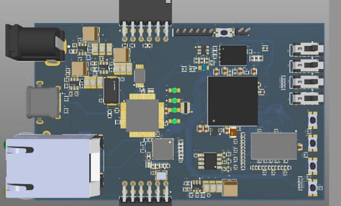
  • 3D PCB renders
  • Drill files & fabrication outputs


Contact me Now

Specialization:

Circuit design

•

Schematics

•

Layout

•

Footprint

File format:

Gerber

•

STEP

•

BRD

•

SCH

•

PDF

Software:

Altium Designer

•

Eagle CAD

•

EasyEDA

•

KiCad

•

LTspice

Interface:

HDMI

•

I2S

•

UART

•

USB

•

SPI

•

I2C

•

SDIO

•

PCIe

•

Wi-Fi

•

BLE

•

BT

•

LTE

•

NB-IoT