Browse categories
Explore
Fiverr Pro
English
$
USD
PCB DESIGN, EMBEDDED SYSTEM AND IOT
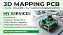
Your 3D mapping project should not fail because sensors, power rails, or high-speed signals were forced onto the wrong PCB architecture. I help turn your LiDAR, camera, IMU, and navigation hardware requirements into a practical board built for real integrationnot just a visually complete schematic.
What Client Will Get
What Makes Me Stand Out
I focus on solving the difficult part: making sensing, processing, power, and communication hardware work together cleanly while considering routing, noise, thermal needs, and future system integration.
Deliverables
Schematic, PCB layout, Gerber/production files, BOM, DRC checks and relevant manufacturing outputs.
Have a 3D mapping or autonomous navigation device in mind? Send your requirements and let's turn them into a production-ready PCB.


Can you integrate LiDAR and camera interfaces on the same PCB?
Yes. I can integrate LiDAR, camera, IMU, MCU/processor, power, and communication interfaces based on your system requirements.
Can you work with high-speed camera or sensor interfaces?
Yes. I can handle appropriate high-speed routing, grounding, layer planning, and signal-integrity considerations for supported interfaces.
Can you create a PCB for autonomous navigation systems?
Yes. I can build the electronics platform for autonomous navigation, including sensing, processing, power, and communication hardware.
What files do I need to provide?
Ideally, provide your system requirements, component preferences, datasheets, reference designs, interface requirements, and mechanical constraints if available.
Will the PCB be ready for manufacturing?
Yes. Depending on the package, deliverables can include schematic, PCB layout, BOM, Gerber files, drill files, and design-rule checks.


