Browse categories
Explore
Fiverr Pro
English
$
USD
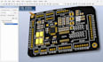
Creating a high performance RF PCB requires precise impedance control, transmission line routing, proper grounding, shielding, and seamless antenna integration. I provide professional RF PCB solutions for wireless, microwave, and high frequency applications using proven engineering practices.
I specialize in RF PCB layout with controlled impedance, microstrip and coplanar waveguide routing, antenna implementation, multilayer stack up planning, and optimized grounding to improve signal integrity and minimize EMI. Every board is developed for reliable performance and efficient manufacturing using Altium Designer and KiCad.
Services I Offer
I develop RF boards for WiFi, Bluetooth, LoRa, GPS, ISM band devices, wireless communication systems, IoT products, and other high frequency applications.
CONTACT NOW and let's get your project started.
What information do you need before starting my RF PCB project?
Please provide your schematic, operating frequency, PCB dimensions, layer count, antenna requirements, component list (BOM), preferred PCB manufacturer, and any impedance specifications.
Can you design PCB antennas?
Yes. I can design PCB antennas and integrate external antenna connectors while following RF layout best practices for improved performance.
Do you design controlled impedance RF PCBs?
Yes. Controlled impedance is one of the most important aspects of RF PCB design. I design transmission lines, microstrip, and coplanar waveguide traces according to your impedance requirements.
Which software do you use?
I primarily use Altium Designer and KiCad for RF PCB layout and manufacturing documentation.
What files will I receive?
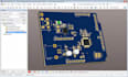
You will receive Gerber files, PCB source files, drill files, Bill of Materials (BOM), Pick and Place files, fabrication drawings, PDF documentation, and a 3D PCB model when required.
Which RF applications do you support?
I support RF PCB designs for WiFi, Bluetooth, LoRa, Zigbee, GPS, ISM band devices, wireless communication modules, IoT products, and other high-frequency electronic systems.
Should I contact you before placing an order?
Yes. RF PCB projects require careful review of frequency, impedance, antenna type, and board stack-up. Contact me before ordering so I can recommend the best package and ensure your project requirements are fully understood.


