Browse categories
Explore
Fiverr Pro
English
$
USD
Advanced PCB Design Engineer for RF IoT AI and Embedded Systems
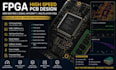
Professional FPGA and high speed PCB design services for compute, telecom, robotics, and embedded hardware systems requiring precise signal integrity and advanced routing control.
My expertise covers FPGA board design, DDR3 DDR4 memory routing, high speed digital interfaces, impedance controlled traces, and multilayer stackup optimization for reliable performance in complex systems.
I design boards with strict focus on signal integrity, timing constraints, EMI reduction, and power integrity across multilayer architectures. This includes differential pair routing, controlled impedance traces, ground reference planning, and noise isolation for high frequency signals.
I work with high speed interfaces such as LVDS, PCIe, Ethernet, and memory buses, ensuring stable FPGA communication and optimized data throughput.
Deliverables include schematic design, PCB layout, Gerber files, BOM, stackup definition, and manufacturing ready documentation. Each design is structured for fabrication readiness and hardware validation.
Ideal for FPGA developers, robotics engineers, telecom hardware, compute systems, and industrial embedded platforms requiring reliable high speed PCB architecture

What FPGA PCB designs do you support?
I design FPGA boards including DDR routing, high speed PCB layout, and multilayer stackup systems.
Do you handle signal integrity and impedance control?
Yes, I specialize in signal integrity, controlled impedance routing, and noise reduction techniques.
Can you design DDR memory interfaces?
Yes, I design DDR3 DDR4 routing with timing alignment, length matching, and optimized trace layout.
What high speed interfaces can you work with?
I design PCIe, Ethernet, LVDS, and other high speed digital interfaces for FPGA systems.
What deliverables will I receive?
You get schematic, PCB layout, BOM, Gerber files, stackup design, and manufacturing ready outputs.
