Browse categories
Explore
Fiverr Pro
English
$
USD
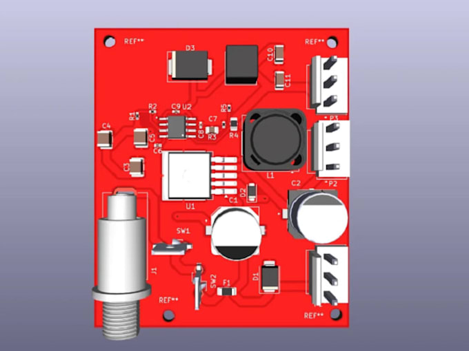
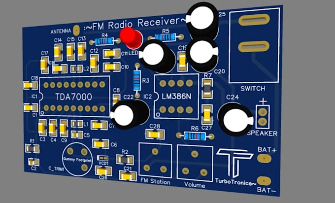
RF PCB Design, High Frequency Layout and Antenna Integration
Need professional high-frequency RF PCB design, antenna layout, and wireless circuit board design for your electronics project?
I provide custom RF PCB layout services for wireless devices, RF modules, and high-frequency electronic products.
WHAT I OFFER:
WHAT I DELIVER:
SOFTWARE USED:
Altium Designer, KiCad, CST Studio Suite, LTspice, Cadence OrCAD, and EasyEDA, depending on project requirements.
Whether you need a high-frequency PCB layout, antenna-integrated board, RF circuit board, or wireless hardware design, I focus on clean routing and manufacturing-ready deliverables.
Contact me before ordering to discuss your operating frequency, board stack-up, antenna requirements, layer count, and project scope.