Browse categories
Explore
Fiverr Pro
English
$
USD
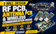
RF PCB, Antenna and IoT Wireless Circuit Design Expert
Hello I'M Ryan Champ Looking for a professional RF PCB, antenna PCB or wireless communication board for your next product? I will design high-performance RF PCB solutions for wireless communication systems with focus on signal integrity, antenna efficiency, reliability and manufacturability.
This gig is perfect for WiFi, Bluetooth, LoRa, GSM, GPS, IoT devices, wireless sensors, tracking systems, embedded electronics and RF communication projects.
What you will get:
Software:
Altium Designer, KiCad, EasyEDA and Eagle PCB.
Deliverables:
Gerber files, BOM, PCB source files, PDF schematics, pick and place files, STEP files, 3D PCB views and manufacturing outputs.
Send your project requirements today and lets create a reliable RF PCB or wireless communication board for your product. I also provide prototype-ready layouts, DFM checks, RF routing optimization, multilayer PCB support and revision assistance for smooth manufacturing and deployment
THANK?

File format:
Gerber
•
STEP
•
BRD
•
SCH
•
ODB
Software:
Altium Designer
•
Eagle CAD
•
EasyEDA
•
KiCad
•
Matlab
•
Proteus
Interface:
UART
•
SPI
•
I2C
•
Wi-Fi
•
BLE
•
BT
•
GSM/GPRS
•
LTE
•
CAT-M1
•
NB-IoT
•
Ethernet
What information do you need to start my RF PCB project?
Please provide your project requirements, schematic, dimensions, operating frequency, preferred components and any reference files.
Can you design antenna PCB and wireless communication boards?
Yes, I design RF PCB, antenna PCB and wireless communication boards for WiFi, Bluetooth, LoRa, GSM, GPS and IoT applications.
What deliverables will I receive?
You will receive Gerber files, BOM, PCB source files, schematics, pick and place files, STEP files and manufacturing-ready outputs.
