Browse categories
Explore
Fiverr Pro
English
$
USD
PCB Design Engineer,Hardware Product Developer,Embedded Systems and RF PCB Exp
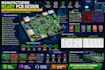
I provide advanced RF PCB design services for wireless communication systems including WiFi, Bluetooth, GSM, GPS, LoRa, Zigbee, and other RF technologies. RF design requires careful planning, impedance control, antenna placement, signal integrity, and EMI management to ensure reliable performance.
I help businesses and startups develop quality wireless products ready for manufacturing.
WHAT I OFFER
Software Used
Used For
Why Choose Me
Contact me now,let discuss your wireless project requirements and receive a tailored solution for your RF product development needs.

Which wireless technologies do you support?
WiFi, Bluetooth, GSM, GPS, LoRa, Zigbee, and RF modules.
Do you design antennas?
Yes, antenna layout and optimization are included.
Can you improve an existing RF design?
Yes, I can review and optimize current designs.
Do you provide manufacturing files?
Yes, all required production files are included.
