Browse categories
Explore
Fiverr Pro
English
$
USD
HELLO AND WELCOME!!!
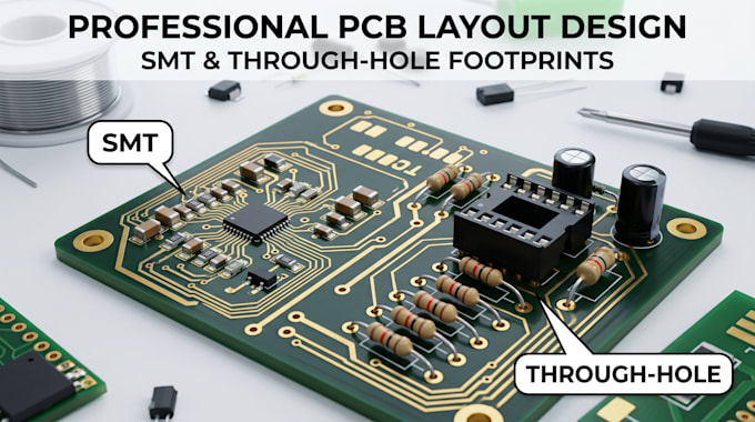
Need a professional PCB layout that is accurate, manufacturable, and optimized for performance? You're in the right place.
I specialize in PCB design and footprint creation for both SMT (Surface Mount Technology) and Through Hole components, delivering production ready files for prototypes and mass manufacturing.
What I Offer:
Why Choose Me?
Tools & Platforms:
Altium Designer, KiCad, EasyEDA, Autodesk Eagle, OrCAD, Proteus, JLCPCB, PCBWay, OSH Park, Fusion 360 Electronics
Message me today and lets turn your circuit idea into a professional PCB ready for manufacturing.


What files do you need to start the PCB design?
I can work with schematics, circuit diagrams, hand-drawn sketches, BOMs, existing PCB files, or detailed project requirements.
Which PCB design software do you use?
I primarily use Altium Designer, KiCad, EasyEDA, Eagle, OrCAD, and Proteus depending on project requirements.
Can you create custom SMT and Through Hole footprints?
Yes. I design custom footprints according to component datasheets and industry standards to ensure manufacturing compatibility.
What deliverables will I receive?
You will receive PCB source files, Gerber files, drill files, BOM, pick and place files, and any other manufacturing documents required.
Can you design multilayer PCBs?
Yes. I can design single layer, double layer, and multilayer PCBs for various applications.
Will the PCB be ready for manufacturing?
Absolutely. All designs undergo DRC checks and are prepared for fabrication services such as JLCPCB, PCBWay, and other manufacturers.