Browse categories
Explore
Fiverr Pro
English
$
USD
Hardware Design , IoT PCB Layout Engineer
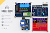
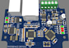
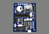
Embedded Systems Engineer with 3+ years experience. I will build iot hardware, smart device pcb layouts, custom pcb architectures using altium designer, and dfm pcb verifications ready for mass fabrication.
Services I Offer:
- Custom IoT hardware design, microcontroller & wireless module integration
- Smart device PCB routing, compact layout, power delivery networks
- Custom PCB schematic capture, component selection, BOM creation
- Multi-layer PCB stackup routing, ground planes, EMI noise mitigation
- Design for Manufacturing (DFM) checks targeting high factory yield
Tools I Use:
Altium Designer, KiCad, Saturn PCB Toolkit.
File Formats Delivered:
Gerber RS-274X/X2, NC Drill, BOM, Centroid Pick-and-Place, Native Altium source files, 3D STEP model, Schematic PDF.
Why Work With Me?
- Unlimited Revisions included across all packages
- DFM rules configured to your target PCB assembly house specs
- Trace geometries calculated for power efficiency and signal integrity
- Turnkey manufacturing assets ready for automated SMT production
Please message me to discuss your project requirements, hardware specs, and component options before placing an order.
What project details should I share prior to starting an IoT hardware order?
Please provide your functional requirements, component datasheets, maximum PCB footprint limits, and target power source. Sharing preliminary block diagrams or hand sketches helps accelerate initial schematic drafting.
Do you complete native project files in Altium Designer?
Yes, I perform multi-layer schematic capture and PCB routing natively in Altium Designer. Full Altium project files (.PcbDoc, .SchDoc, libraries) are included in standard and premium tiers.
How does DFM PCB checking benefit my manufacturing run?
Design for Manufacturing (DFM) verifies annular rings, trace clearances, solder mask expansions, and silkscreen overlays against your fabricator's capabilities. This eliminates costly factory floor hold-ups and increases production yield.
Can you build custom PCB layouts for high-density smart device products?
Yes, I route high-density smart device PCB layouts using micro-vias, compact SMT packages (0402/0201), and multi-layer stackups tailored for space-constrained consumer electronics.
Will the output package contain everything needed for automated SMT fabrication?
Absolutely. You receive complete Gerber RS-274X/X2 sets, NC Drill files, bill of materials (BOM), and Pick-and-Place XY centroid coordinates formatted for assemblers like JLCPCB, PCBWay, or local SMT lines.
How are Unlimited Revisions handled during project execution?
: Unlimited Revisions cover adjustments to component layouts, trace rerouting, board edge modifications, and manufacturing file adjustments within the agreed initial project scope.


