Browse categories
Explore
Fiverr Pro
English
$
USD
Got a circuit that needs to become a real PCB?
I design custom PCB layouts from schematics, circuit diagrams, or existing designs, with the focus on getting the board properly prepared for fabricationnot simply placing components and connecting traces.
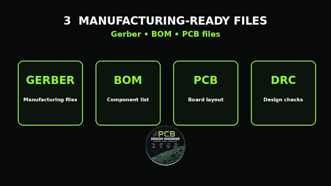
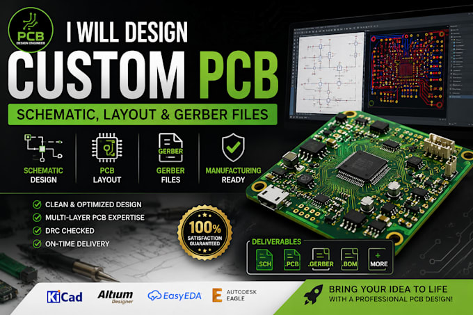
I can handle PCB schematic capture, component placement, routing, 2-layer and multilayer layouts, footprint selection, design-rule checks, Gerber/NC Drill generation, BOM preparation, and 3D PCB views.
Projects can include ESP32, STM32, Arduino, IoT, sensor boards, controllers, power electronics, USB boards, embedded hardware, and custom electronic products.
Your design is developed around the actual board requirements: component availability, board dimensions, connector positions, mounting holes, layer stack-up, routing constraints, and manufacturer requirements.
Depending on the package, you can receive the editable source files, schematic, PCB layout, BOM, Gerber files, NC Drill files, and fabrication-ready documentation.
If you already have a schematic, send it to me. If you only have a circuit concept or existing PCB that needs redesigning, message me first so I can assess the scope and recommend the appropriate package.
Specialization:
Circuit design
File format:
Gerber
Software:
Altium Designer
•
Eagle CAD
•
KiCad
•
NI Multisim
Interface:
USB
Can you design a PCB from an existing schematic?
Yes. I can use your existing schematic as the basis for component placement, PCB layout, routing, and manufacturing-ready files.
Can you create the schematic too?
Yes. Schematic design is included in the Standard and Premium packages. Please contact me first if your project requires a complex schematic.
Do you provide Gerber files?
Yes. Fabrication-ready Gerber files are included according to the selected package.
Can you design multi-layer PCBs?
Yes. Multi-layer PCB design is available in the Standard and Premium packages, with the maximum layer count depending on the package selected.