Browse categories
Explore
Fiverr Pro
English
$
USD
PCB Design and Embedded Systems Engineer
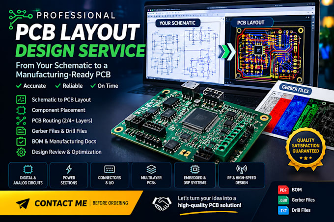
Do you have a completed schematic that needs to be converted into a professional, organized, and manufacturing-ready PCB?
I will convert your schematic or circuit diagram into a complete PCB layout according to your component specifications, board requirements, and project needs.
What I can provide:
Suitable for:
Please message me before placing an order, especially for complex, multilayer, high-speed, RF, or specialized PCB projects. Send your project requirements so I can review the scope and recommend the appropriate package.
Can you convert my schematic into a PCB layout?
Yes. I can create the PCB layout from your schematic and available component information.
What files should I provide?
You can provide your schematic, component list, datasheets, board dimensions, layer requirements, and any reference files available.
Do you provide Gerber files?
Yes. Gerber and drill files can be included according to the selected package.
Can you work with existing PCB projects?
Yes. I can modify, optimize, or update an existing PCB layout when the project files are available.