Browse categories
Explore
Fiverr Pro
English
$
USD
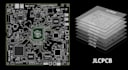
Hi! I will design high speed or multilayer PCB layout, schematic, and Gerber files ready for JLCPCB.
Specialized in professional high-speed and multilayer PCB designs (4 to 8 layers) with proper signal integrity and manufacturing optimization.
What you get:
Specialties:
Tools: KiCad & Altium Designer
I deliver clean, reliable, and manufacturable files that work well on JLCPCB.
Send your schematic, block diagram, or requirements (speed, layers, interfaces) Ill provide JLCPCB-ready files with fast delivery and revisions until perfect.
Message me with your project details for a quick quote!


Are the files ready for JLCPCB?
Yes — I design specifically with JLCPCB capabilities and stack-up in mind.
Do you handle high-speed signals?
Yes, I specialize in impedance control, differential pairs, and length matching.
Can you design 6 or 8 layer boards?
Absolutely, multilayer design is one of my main specialties.
Do you provide stack-up recommendations?
Yes, included in all packages.


