Browse categories
Explore
Fiverr Pro
English
$
USD
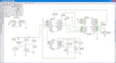
Turn your idea, sketch, or requirements into professional, manufacturable PCB files fast. I specialize in clean schematics, optimized layouts, and full production packages that pass JLCPCB's checks with zero issues.
What you get:
Ideal for prototypes, IoT, embedded, consumer electronics, sensors, power boards hobbyists, startups, engineers.
I ensure files are JLCPCB-optimized (panelization notes, solder mask, silkscreen, etc.) so you can order directly without revisions.
Message me your specs (size, layers, components, special needs like high-speed/power/thermal) quick response & start from scratch!
Unlimited chat + support after delivery. Let's get your board fabricated hassle-free!


File format:
Gerber
•
STEP
•
VRML
•
SCH
•
ODB
Software:
Allegro
•
EasyEDA
•
Fusion 360
•
KiCad
•
LTspice
•
PLECS
Interface:
HDMI
•
MIPI DSI/CSI
•
I2S
•
USB
•
SPI
•
I2C
•
SDIO
•
Wi-Fi
•
BLE
•
Ethernet
Are the files ready for direct JLCPCB upload?
Yes – Gerber, Drill, BOM, Pick & Place optimized for JLCPCB (tested compatibility).
What software do you use?
KiCad (primary), Altium Designer, Eagle/Autodesk – flexible based on your needs.
Can you handle multilayer or high-speed designs?
Yes, up to 8+ layers with proper stackup and checks.
Do you help with JLCPCB ordering?
Premium includes guidance; I can review quotes/files before you order.
NDA available?
Yes – sign for any confidential project.
After-delivery support?
Free for minor fixes/adjustments.


