Browse categories
Explore
Fiverr Pro
English
$
USD
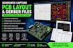
I specialize in schematic capture, PCB layout design, and complete manufacturing file preparation for embedded systems, IoT devices, consumer electronics, industrial hardware, automation systems, and custom electronic products.
Whether you need a simple prototype PCB or a complex multilayer board, I will provide clean, efficient, and fabrication-ready designs optimized for performance and manufacturing.
SERVICES I OFFER:
I focus on delivering professional and manufacturing-ready PCB designs optimized for reliability and performance.


What files will I receive?
You will receive Gerber files, PCB layout files, schematic files, BOM, and manufacturing-ready outputs.
Which PCB software do you use?
I use Altium Designer, KiCad, and Eagle for PCB development.
Do you provide multilayer PCB design?
Yes, I design both simple and complex multilayer PCBs
Can you redesign an existing PCB?
Yes, I can redesign and optimize existing PCB layouts.
Will the PCB be ready for manufacturing?
Yes, all files will be optimized for PCB manufacturers like JLCPCB and PCBWay.
Do you perform DRC checks?
Yes, all PCB layouts are checked for manufacturing and routing errors.
Can you create PCB from hand-drawn sketches?
Yes, I can convert sketches or ideas into professional schematics and PCB layouts.
Do you support IoT and embedded systems?
Yes, I work on embedded systems, IoT devices, and automation hardware.
Can you provide BOM files?
Yes, BOM preparation is included for component sourcing and assembly.
Can you help from idea to prototype?
Yes, I can assist throughout the complete PCB development process.


