Browse categories
Explore
Fiverr Pro
English
$
USD
ELECTRICAL AND ELECTRONICS ENGINEERING
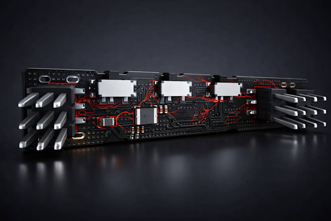
Hi, Im Daniel, and I specialize in professional PCB design, PCB layout, schematic capture, and Gerber files for your electronics projects. From prototypes to production-ready boards, I deliver high-quality, manufacturable designs using Altium, KiCad, or EasyEDA.
You get complete deliverables:
Supported projects / technologies:
Why choose me:
Ready to turn your idea into a working PCB?
Message me Now and lets build something amazing!

File format:
Gerber
•
STEP
•
BRD
•
SCH
•
Software:
Altium Designer
•
DipTrace
•
Eagle CAD
•
EasyEDA
•
KiCad
Interface:
UART
•
USB
•
SPI
•
I2C
•
Wi-Fi
•
BLE
•
Ethernet
What do I get with your PCB design service?
You get a complete PCB package: schematics, multi-layer layout, Gerbers, BOM, pick-and-place files, and optional 3D models—all manufacturing-ready and following industry DRC/ERC and DFM standards.
Which platforms and boards do you support?
I work with Altium, KiCad, and EasyEDA for embedded systems, ESP32, Arduino, STM32, IoT, and high-speed electronics. Designs are optimized for signal integrity, routing, and first-time assembly success.
Why choose your PCB design service?
I deliver reliable, manufacturable PCBs, avoiding EMI or grounding issues. Fast turnaround, unlimited revisions, and clear communication ensure your project is smooth and professional.