RF PCB Designer Antenna Integration and Controlled Impedance
United States
English
About me
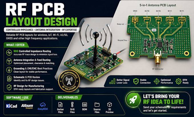
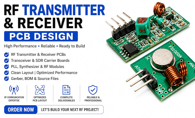
I am an RF PCB design specialist focused on helping engineers, startups, and product developers turn electronic concepts into manufacturable PCB layouts. My services include RF PCB layout, controlled impedance routing, antenna integration, schematic review, grounding checks, and PCB design correction. I support Wi-Fi, Bluetooth, IoT, and RF communication projects based on your requirements. I aim to deliver organized design files, clear communication, and reliable project support. Contact me to discuss your project scope, technical needs, and manufacturing goals before ordering.... Read more