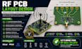
I will design rf pcb layout, antenna integration and controlled impedance routing

United States

I speak English

RF PCB Designer Antenna Integration and Controlled Impedance

I am an RF PCB design specialist focused on helping engineers, startups, and product developers turn electronic concepts into manufacturable PCB layouts. My services include RF PCB layout, controlled ...
About this Gig

Need reliable RF PCB design for your wireless, antenna, IoT, or RF communication product? I can help you create or improve your PCB layout and prepare it for manufacturing.


I provide RF PCB design services for engineers, startups, and product developers who need better routing, controlled impedance, and reliable high-frequency performance.


MY SERVICES

  • RF PCB layout and routing
  • Controlled impedance design based on your required specifications and PCB stackup
  • Antenna integration and feed routing
  • Schematic and existing PCB layout review
  • Grounding, signal integrity, and EMI/EMC design checks
  • RF matching network implementation, where applicable
  • Fabrication-ready Gerber, drill, BOM, and other agreed files


PROBLEMS I HELP ADDRESS

Poor RF routing can increase signal loss. Incorrect impedance can cause signal reflections. Poor grounding and component placement can contribute to interference. I review these design areas and apply appropriate layout practices to help reduce potential issues before fabrication.


WHAT YOU RECEIVE

  • Editable files in [KiCad/Altium/EasyEDA]
  • PCB layout or review based on your project scope
  • Manufacturing files and design notes as agreed


LET'S DISCUSS YOUR PROJECT

Specialization:

Circuit design

•

Schematics

•

Layout

•

Footprint

File format:

Gerber

•

STEP

•

PDF

•

ODB

•

Circ

Software:

EasyEDA

•

Fusion 360

•

KiCad

•

Matlab

•

Proteus

•

SolidWorks

Interface:

HDMI

•

I2S

•

UART

•

USB

•

SPI

•

SDIO

•

PCIe

•

Wi-Fi

•

BLE

•

BT

•

GSM/GPRS

•

LTE