d
david__ryan_

David R

@david__ryan_

Professional PCB Design, Altium and KiCad, Fabrication Ready Boards

United Kingdom
English, Spanish, French, German, Italian
About me
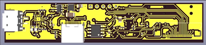
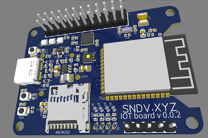
Electronics engineer specializing in professional PCB design and schematic development using Altium Designer and KiCad. I help startups, engineers, and makers turn ideas into fabrication-ready circuit boards with clean layouts, optimized routing, and complete manufacturing files. My services include schematic capture, multi-layer PCB layout, Gerber generation, BOM preparation, and 3D board rendering. I focus on reliability, clear communication, and on-time delivery so your hardware project moves smoothly from concept to production.... Read more

Skills

d
david__ryan_
David R
Offline • 
Average response time: 1 hour

See my services

Printed Circuit Boards (PCB)
I will design iot rf pcb and layout using altium or kicad for wireless antenna devices
Printed Circuit Boards (PCB)
I will design raspberry pi pcb, cm4 cm5 carrier board hat with gerber bom 3d and files