Browse categories
Explore
Fiverr Pro
English
$
USD
Expert PCB Designer Schematic, Multilayer, RF, ESP32, Arduino PCB Layout
Need an RF PCB that performs reliably at high frequencies? Poor routing, impedance mismatch, EMI, and weak antenna performance can turn a working circuit into a costly prototype problem.
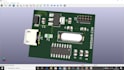
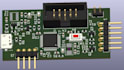
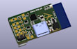
I provide professional RF PCB design, simulation, antenna design, RF layout, and high speed PCB layout for wireless and embedded hardware projects.
What You Get
Software I Use
Altium Deslgner, KiCad, HFSS, ADS and related RF/PCB tools.
Files & Deliverables
Schematic, PCB source files, Gerbers, drill files, BOM, drawings, simulation results, and deslgn documentation as required.
Why Choose Me
I focus on practical RF engineering, clean layouts, impedance matching, manufacturability, and reliable hardware performance.
Ready to build your RF or high speed PCB?
Contact me with your requirements, schematic, specifications, or existing files before placing order.
What files will I receive?
Depending on the package, you can receive PCB source files, schematics, Gerbers, drill files, BOM, drawings, and simulation results.
Can you design RF antennas?
Yes I can work on PCB antenna layouts and RF antenna designs for wireless applications such as WiFi, BLE, GPS, LoRa, and IoT.
Can you work with my existing PCB?
Yes I can review, modify, optimize, or continue an existing Altium or KiCad design.
What do you need before starting?
Please provide your schematic or block diagram, board dimensions, components, frequency requirements, layer stackup, antenna requirements, and any existing files.
Do you provide HFSS or ADS simulation?
Yes, when included in the selected package. Simulation scope depends on the RF structure and project requirements.
Do you provide revisions?
Yes Revisions are included according to the selected package. Major design changes outside the original scope may require a custom offer.
Will you keep my project confidential?
Yes I treat client project information and design files as confidential and will not publicly share proprietary project details.


