d
david_rappaport

David Rappaport

@david_rappaport

Expert Schematic and PCB Design Engineer

United States
English, French, German, Spanish
About me
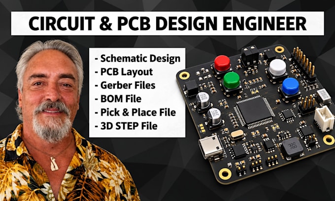
PCB Design Expert specializing in professional schematic design, PCB layout, routing, and board optimization. I work with Altium Designer and KiCad to create reliable, production-ready PCB designs, including multi-layer, rigid-flex, RF, and embedded systems. I can handle projects from schematic reconstruction and component selection to layout, DRC validation, Gerber generation, BOM preparation, and manufacturing-ready source files. My focus is on accuracy, clean design, and practical engineering solutions.... Read more

Skills

d
david_rappaport
David Rappaport
Offline • 
Average response time: 1 hour

See my services

Printed Circuit Boards (PCB)
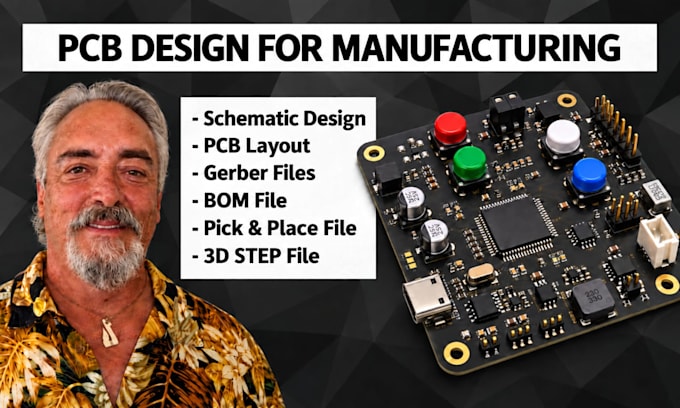
I will design circuit schematic and pcb layout ready for jlcpcb or pcbway manufacturing
Printed Circuit Boards (PCB)
I will design circuit schematics and pcb layout in easyeda, altium or eagle kicad

Work experience

IOTA_Engineering

PCB Designer

IOTA Engineering • Full-time

Aug 2015 - Present11 yrs 1 mo

I specialize in the use of Altium Design Tools V15,V16, V17 and have my own software license. I also have P-CAD, OrCad, and PADS software at my disposal. I have over 10 years of experience using Altium(23+ years designing PCB’s) and have successfully created designs of up to 26 layers incorporating mixed signal technologies, split plane architecture, high speed, matched length buses/differential pairs, DDR3 Ram, PCIe and USB 3.0 interfaces, switching and linear power supply architecture. I have also created and maintained numerous Design Libraries. I work with both Electrical and Mechanical Engineers to ensure that all designs meet both in-house and customer specifications