Browse categories
Explore
Fiverr Pro
English
$
USD
Turning your idea into a working circuit board takes more than just connecting wires it needs an engineer who understands signal integrity, power distribution, and manufacturability from day one.
As an Electrical Engineering student specializing in power systems, I design clean, manufacturable schematics and PCB layouts that just work the first time.
What I offer:
Ideal for:
IoT devices, sensor boards, power converters, Arduino/ESP32 shields, breakout boards, prototypes, and student/hobbyist projects.
I combine formal EE training with hands-on design experience to deliver boards that pass DRC/ERC clean and are ready to manufacture no revisions wasted on preventable errors
.
Message me with your circuit requirements before ordering for an accurate quote and timeline.

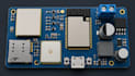
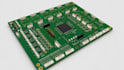
Specialization:
Circuit design
•
Schematics
•
Layout
File format:
Gerber
•
STEP
•
BRD
•
SCH
•
Software:
Altium Designer
•
EasyEDA
•
KiCad
I only have a rough sketch/idea, not a finished schematic — can you still help?
Absolutely. I can take a hand-drawn concept, a datasheet reference design, or even just a functional description and turn it into a proper schematic from scratch.
Will the PCB be ready to send straight to manufacturing?
Yes. You'll receive Gerbers, drill files, BOM, and pick-and-place files — fully DRC/ERC checked and formatted for fabs like JLCPCB and PCBWay.
Can you design multi-layer boards?
Yes, I handle 2-layer through multi layer designs, including proper stackup planning and impedance-controlled routing where needed.
Do you work with both KiCad and EasyEDA?
Yes — I'm fully proficient in both. I'll recommend whichever fits your project and fab house best, or use whichever you already have files in.


