Browse categories
English
$
USD
Connect to your AI
Need a custom ESP32 or IoT PCB for your electronics project?
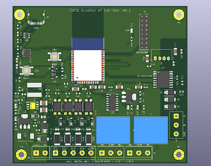
I will design a 2-layer PCB in KiCad based on your circuit requirements or existing schematic, with a focus on clean layout, organized component placement, and practical routing.
What I can provide:
Why work with me?
Before ordering: Please share your schematic or circuit requirements, required components, board dimensions, and any special constraints. Contact me before ordering if your project involves complex circuitry or specific manufacturing requirements.
I will work carefully to deliver a well-organized design within the agreed scope. Advanced electrical validation, certification, and guaranteed manufacturing performance are not included unless explicitl


Specialization:
Circuit design
•
Schematics
•
Gerber
File format:
Gerber
•
SCH
•
3DS
Software:
KiCad
What do you need from me to start?
Please provide your schematic or circuit requirements, component list, preferred board dimensions, and any special design constraints. Reference designs and component datasheets are helpful too.
Can you design a PCB from my idea without a schematic?
Yes, if you provide clear circuit requirements and component details. The complexity of the project will determine whether it fits your selected package, so please contact me first.
Which files will I receive?
Deliverables depend on your package. They may include the schematic, routed PCB layout, BOM, Gerber and drill files, and KiCad source files. Please check your package details before ordering.
Do you check the design for errors?
I perform applicable KiCad ERC/DRC checks within the agreed scope and address identified issues where possible. These checks do not guarantee that the circuit will function correctly or pass every manufacturing test.
Do you provide a BOM and 3D PCB render?
Yes. The BOM is included in Standard and Premium, while the 3D render and complete KiCad source files are included in Premium, as specified in the packages.
Can you guarantee the PCB will work perfectly?
I carefully check the design within the agreed scope, but I cannot guarantee flawless hardware operation or certify advanced electrical, RF, impedance, or manufacturing requirements. Complex projects should be discussed before ordering.
Can you design boards with more than two layers?
My standard packages cover 2-layer PCBs. If you need a multilayer board or a design with advanced routing constraints, please contact me first to discuss feasibility and pricing.