Browse categories
Explore
Fiverr Pro
English
$
USD
Professional PCB Design for Reliable Electronics
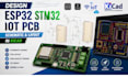
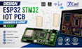
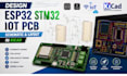
Need a reliable PCB for your ESP32, STM32, IoT or embedded electronics project?
I will design a professional PCB schematic and layout in KiCad based on your requirements, reference circuit or existing design. I can help with component selection, schematic capture, PCB placement, routing, power and signal connections, design-rule checks and manufacturing-ready files.
What I can deliver:
Tools:
I focus on clean layouts, practical routing and production-ready documentation. Send your circuit requirements, schematic, datasheet or reference design and Ill turn your concept into a professional PCB.
Message me before ordering if your project is complex or requires a custom scope.
Can you design ESP32 and STM32 boards?
Yes. I can design custom boards around ESP32, STM32 and other embedded controllers.
Can you work from an idea instead of a schematic?
Yes, depending on the project. Send your requirements and I can determine the appropriate workflow.
Do you provide Gerber files?
Yes, when included in your selected package.
Can you create multilayer PCBs?
Yes. Multilayer designs can be included depending on project complexity.
Can you work with an existing PCB?
Yes. I can review, modify or improve existing PCB designs.


