Browse categories
Explore
Fiverr Pro
English
$
USD
Looking for an experienced RF PCB designer to develop reliable high-frequency circuits and antenna solutions? I provide professional RF PCB design services for wireless communication, IoT devices, embedded systems, and research applications that require excellent signal performance and manufacturing accuracy.
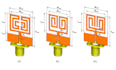
I design RF circuit boards with careful attention to impedance control, transmission lines, grounding, isolation, and layout techniques that reduce interference while maximizing efficiency. Whether you need a microstrip PCB, patch antenna, RF front-end, matching network, or a complete wireless hardware solution, I deliver optimized designs ready for fabrication.
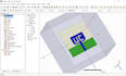
My services include RF PCB layout, antenna design, microstrip and stripline routing, impedance matching, HFSS simulation, CST simulation, schematic review, multilayer PCB design, Gerber generation, BOM preparation, design rule checks, and production-ready documentation.
Why work with me?
CONTACT NOW LETS GET YOUR PROJECT STARTED.
What RF PCB design services do you provide?
I design RF PCBs, patch antennas, microstrip layouts, matching networks, wireless modules, and high-frequency circuit boards for commercial, industrial, and research applications
Can you design custom antennas?
Yes. I design patch antennas, microstrip antennas, PCB antennas, and other custom antenna solutions based on your operating frequency, bandwidth, and application requirements.
Which simulation software do you use?
I use Ansys HFSS and CST Studio Suite for electromagnetic simulation, antenna analysis, impedance matching, and RF performance optimization.
What files will I receive?
You will receive PCB source files, Gerber files, BOM, drill files, Pick and Place files, assembly drawings, and other manufacturing documents included in your package.
Can you optimize an existing RF PCB?
Absolutely. I can review your current RF PCB layout, improve impedance matching, reduce signal loss, minimize interference, and enhance antenna performance.
Do you design multilayer RF PCBs?
Yes. I design multilayer RF PCBs with controlled impedance, proper grounding strategies, RF shielding considerations, and optimized stack-up planning.
What information do you need before starting?
Please provide your schematic, operating frequency, substrate preference, board dimensions, antenna specifications, mechanical constraints, and any performance requirements. If you only have an idea, I can help develop the design.


