Browse categories
Explore
Fiverr Pro
English
$
USD
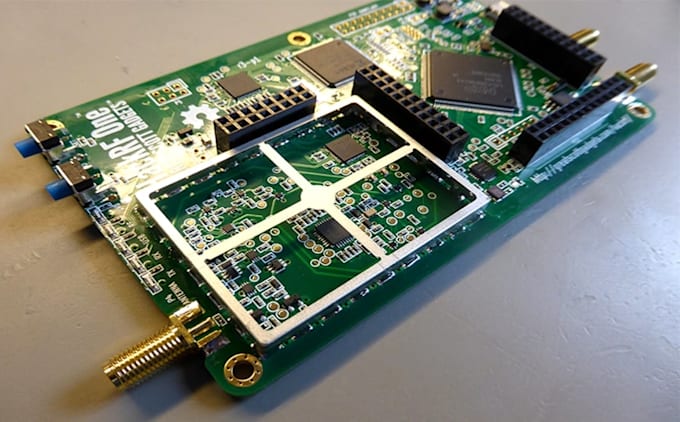
Are you looking for a professional RF PCB layout for a transceiver circuit or wireless communication system? I can help transform your circuit schematics into organized, manufacturable printed circuit board layouts with attention to signal integrity, impedance control, grounding, and high frequency performance.
I specialize in RF PCB layout development for wireless electronics, radio frequency circuits, and communication hardware using industry standard PCB design tools.
MY SERVICES INCLUDE:
APPLICATIONS
Contact me before ordering if your project, Let's turn your RF circuit requirements into a practical PCB layout for your wireless communication


Which PCB design software do you use?
I work with Altium Designer, KiCad, and Cadence Allegro, depending on the project requirements.
Can you develop layouts for RF transceiver circuits?
Yes. I can work on transmitter, receiver, RF front-end, and transceiver PCB layouts based on the supplied schematic and technical specifications.
Do you support impedance controlled routing?
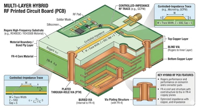
Yes. Controlled-impedance routing can be incorporated when the target impedance, PCB stack-up, dielectric properties, and fabrication constraints are available