Browse categories
Explore
Fiverr Pro
English
$
USD
Electrical Engineer and PCB Layout Designer, Electronics Prototyping
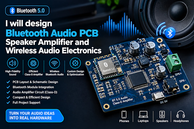
Need a noise-free Bluetooth audio PCB or custom speaker amplifier circuit? As an electronics engineer, I specialize in professional hardware layout and high-fidelity routing for wireless audio electronics. Whether you are building a portable Bluetooth speaker, an amplifier board, or a smart audio system, I deliver clean, production-ready results.
Audio circuits require expert layouts. My process focuses on strict signal isolation, low-distortion paths, and optimal power management to eliminate background current hum, pop noises, and RF interference.
My service includes custom schematic development, multi-layer board creation, and seamless Bluetooth audio module integration. I handle audio amplifier circuit engineering for Class D, Class A/B, or TPA series hardware while implementing low-noise routing to maximize signal integrity.
Final delivery provides complete Gerber files, a comprehensive Bill of Materials (BOM) with sourcing links, circuit schematic diagrams, and a 3D STEP file for enclosure fitting.
I work in Altium Designer, KiCad, and EasyEDA. Please click 'Contact Me' to discuss your specs before ordering.
Specialization:
Circuit design
•
Layout
•
Gerber
File format:
Gerber
•
STEP
•
SCH
•
Software:
Altium Designer
•
Eagle CAD
•
EasyEDA
•
KiCad
Interface:
I2S
•
UART
•
USB
•
SPI
•
I2C
•
Wi-Fi
•
BT
