Browse categories
Explore
Fiverr Pro
English
$
USD

PCB Design and Electronics Engineer
Skills
See my services

PCB Design & Layout Engineer
Cadworld • Full-time
Apr 2025 - Jul 2026 • 1 yr 3 mos
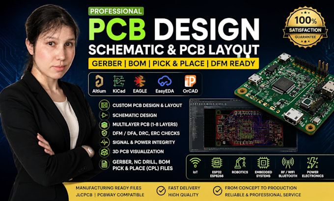
Designed custom, professional, and manufacturing-ready PCB designs, PCB layouts, and circuit schematics for electronics, embedded systems, IoT, robotics, sensor, consumer electronics, industrial control, and power electronics applications. Developed PCB projects from concept and schematic capture through component selection, placement, routing, design verification, and fabrication-ready documentation. Experienced with Altium Designer, KiCad, Eagle, EasyEDA, and OrCAD, creating single-layer, 2-layer, 4-layer, and multilayer PCB layouts with clean routing, ground planes, copper pours, stitching vias, and optimized component placement. Worked with digital, analog, mixed-signal, RF, WiFi, Bluetooth, and high-speed PCB designs, including signal integrity, power integrity, differential pair routing, and impedance-controlled routing where required. Prepared complete manufacturing packages including Gerber files, NC drill files, BOM (Bill of Materials), Pick & Place/CPL files, and 3D PCB models. Performed DRC, ERC, DFM, DFA, and manufacturing checks to help ensure reliable fabrication and assembly. Designed boards compatible with manufacturers such as JLCPCB and PCBWay, with focus on manufacturability, performance, accuracy, and production readiness. Also worked on ESP32, ESP8266, IoT, embedded systems, robotics, RF, power electronics, and hardware prototyping, transforming ideas and schematics into reliable custom PCB solutions.

PCB Design, Electronics Engineering, and Prototyping:
Newbury Electronics Ltd • Full-time
May 2023 - Jun 2024 • 1 yr 1 mo
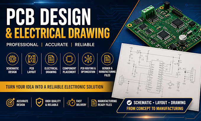
Designed schematic circuits and PCB layouts for embedded and electronic projects. Developed single-layer, double-layer, and multi-layer PCB boards using industry-standard EDA tools. Generated manufacturing-ready Gerber files, BOMs, and assembly documentation. Selected electronic components based on performance, availability, and cost requirements. Worked on microcontroller-based systems including STM32, ESP32, Arduino, and IoT devices. Performed PCB routing, signal integrity optimization, and design verification. Supported prototyping, testing, troubleshooting, and hardware validation. Collaborated with clients to transform project requirements into reliable electronic solutions. Delivered professional electrical drawings, wiring diagrams, and technical documentation. Assisted in product development from concept, schematic capture, PCB layout, and prototype testing to final production.
