Browse categories
Explore
Fiverr Pro
English
$
USD
Electronic and Electrical Engineer
Are you struggling with RF PCB design, antenna layout, wireless communication issues, signal integrity problems, impedance matching, EMI/EMC failures, poor RF performance, or unreliable IoT device connectivity?
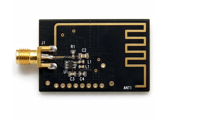
I provide professional RF PCB design services for WiFi, Bluetooth, BLE, LoRa, GPS, GSM, RFID, NFC, UHF, microwave, and wireless IoT devices.
I specialize in RF circuit design, antenna PCB design, impedance controlled routing, high frequency PCB layout, multilayer RF PCB, controlled impedance PCB, signal integrity optimization, RF simulation, and production-ready PCB development.
Whether you need a custom IoT device, wireless sensor, GPS tracker, LoRa gateway, BLE product, smart home device, industrial IoT hardware, or RF communication system, I deliver optimized schematics, PCB layouts, Gerber files, BOM, DFM review, manufacturing support, and prototype-ready solutions.
My designs focus on maximum RF performance, stable wireless connectivity, reduced noise, EMI/EMC compliance, efficient antenna placement, and reliable product manufacturing.
Contact me today and let's transform your RF concept into a high-performance wireless product.
What information do you need to start my RF PCB project?
I need your project requirements, operating frequency, wireless protocol (WiFi, BLE, LoRa, GPS, RFID, GSM), power requirements, and any reference design if available.
Can you design RF PCBs with antenna layout and impedance control?
Yes. I specialize in RF PCB design, antenna layout, controlled impedance routing, signal integrity optimization, and wireless communication systems.
Do you provide Gerber files, BOM, and manufacturing-ready outputs?
Yes. You will receive complete production-ready files including schematics, PCB layout, Gerber files, BOM, and manufacturing documentation.
Can you design RF PCBs for WiFi, Bluetooth, LoRa, GPS, and IoT devices?
Absolutely. I design RF and wireless PCBs for IoT products, GPS trackers, LoRa devices, BLE products, WiFi systems, RFID applications, and industrial wireless solutions.
How do you ensure reliable RF performance?
I follow RF design best practices including antenna optimization, impedance matching, signal integrity analysis, EMI/EMC considerations, and proper PCB stack-up design for stable wireless performance.
