Browse categories
Explore
Fiverr Pro
English
$
USD
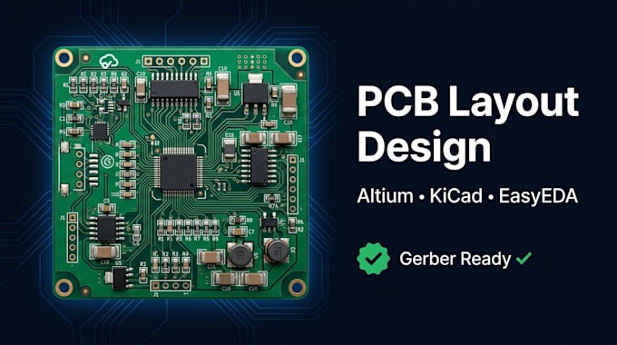
Embedded Systems Engineer Schematic and PCB Layout Specialist
Are you building a product, prototype, or hobby project and need a
clean, manufacture-ready PCB layout? You've found the right designer.
I design professional PCB layouts and schematics using Altium Designer
and KiCad delivering boards that pass DRC checks, route efficiently,
and are ready to manufacture at JLCPCB, PCBWay, OSH Park, or any
fab house of your choice.
WHAT I DELIVER
TOOLS & EXPERTISE
Board types I've designed:
Contact me now!

Which EDA software do you use?
I primarily use Altium Designer and KiCad. I also work in EasyEDA and Eagle. Let me know your preferred tool and I'll match it.
Do you design the schematic or just the PCB layout?
Both. The Standard and Premium packages include full schematic design. If you already have a schematic, I can work from your existing file and proceed directly to layout.
What files will I receive?
At minimum you receive Gerber files (all copper, mask, silkscreen, edge cuts), drill files, and a BOM. The Premium package also includes source files (KiCad .kicad_pcb or Altium .PcbDoc) so you can modify the design yourself later.
Can you design high-speed or RF boards?
Yes. I handle impedance-controlled traces, proper ground plane design, differential pair routing, and antenna placement. Select the RF/High-Speed Review extra for a dedicated signal integrity check.
Will the files be ready to upload directly to JLCPCB or PCBWay?
Yes. All Gerber files are formatted for direct upload to JLCPCB, PCBWay, OSH Park, and other major PCB fabrication services. I include manufacturing notes in the Premium package.
