Browse categories
English
$
USD
Connect to your AI
3D CAD Designer, SolidWorks and Fusion 360 Expert
Level 1
Has met certain performance criteria and shows strong potential in the marketplace.
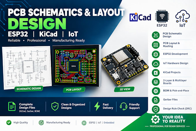
Need a professional PCB schematic and layout for your electronics, ESP32, or IoT project?
I design PCB schematics and PCB layouts using KiCad, with a focus on clean circuit design, accurate connections, practical board layouts, and manufacturing ready files. Whether you have an existing circuit, rough concept, or complete project requirements, I can help turn it into a structured PCB design.
SERVICES I OFFER
WHAT YOU'LL RECEIVE
WHY CHOOSE MY SERVICE?
Please contact me before ordering, especially for complex boards or custom ESP32/IoT projects, so we can confirm the requirements, board layers, components, and deliverables.