Browse categories
Explore
Fiverr Pro
English
$
USD
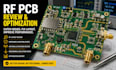
Need an RF PCB reviewed before fabrication? I inspect RF layouts to identify issues in routing, grounding, impedance planning and antenna connections before costly revisions.
WHAT I CAN DO
BENEFITS YOULL GET
Get clear engineering findings and practical next stepsnot vague feedback.
I assess your design against its frequency, components, stackup and manufacturing constraints, helping catch layout risks early and prepare for the next development stage.
TOOLS I WORK WITH
I use KiCad or Altium and can provide annotated feedback, revised PCB files and relevant manufacturing outputs, depending on scope.
Send your PCB project, schematic, target frequency, stackup or fabricator details, and known issues.
I'll confirm scope before starting. Review does not guarantee RF performance; simulation, lab testing and certification are excluded unless agreed separately.
Can you review an existing RF PCB without redesigning the whole board?
Yes. I can assess your current layout and identify concerns first. If only specific areas need changes, we can agree on targeted corrections rather than redesigning the entire PCB.
Can you review 2.4 GHz and 5 GHz Wi-Fi PCB layouts?
Yes, where the project falls within my confirmed capabilities and the necessary design information is available. Please share the target frequency, RF components, stackup and antenna details before ordering.
Can you check 50-ohm impedance and RF routing?
I can review routing against the specified impedance target, PCB stackup and fabrication information. A layout review alone does not constitute a measured or independently verified impedance result.
What files do you need to begin?
Ideally, send the editable PCB project, schematic, component datasheets, stackup information, target frequency, antenna details and PCB manufacturer specifications. Screenshots can help explain the problem but may not be sufficient for corrections.
Will you provide corrected files and a report?
Yes, when included in your selected package. The deliverables will be agreed before work begins. RF simulation, laboratory testing, certification and guaranteed wireless performance are not included unless separately agreed.


