Browse categories
English
$
USD
Connect to your AI
Mechatronics Engineering Expert
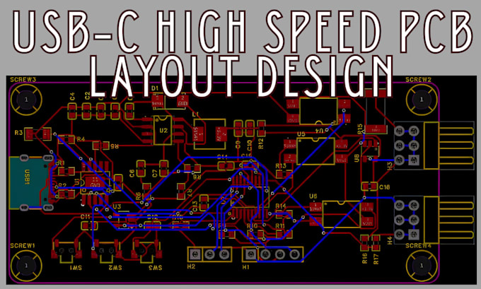
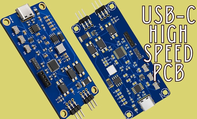
Your USB-C board needs the pairs routed to the right impedance and files your fab accepts the first time. That is the work I do.
Send me your schematic and the USB controller part number. I read the impedance target in the datasheet and match your fab's listed stackup. Then I calculate trace width and spacing and route the USB 2.0 or USB 3.x pairs with length matching and a clean ground return. The USB-C parts get the same attention: CC resistors and ESD protection next to the connector, plus a power delivery circuit if you need one.
What you receive:
I work in KiCad or Altium and can follow JLCPCB or PCBWay rules. Impedance is calculated on the fab's stackup. Only the fab can measure the finished board, so ask it for a test coupon if you need proof. USB-IF certification is not included.
Message me before ordering with your schematic and fab, and I will quote a fixed price.
Which USB speeds do you route?
USB 2.0 and USB 3.x pairs on USB-C boards, including 5 and 10 Gbps links. USB4 and Thunderbolt 5 at 40 to 120 Gbps need retimers and extra work, so ask first and I will tell you if I can take it.
What impedance target do you use?
The one in your controller's datasheet. Guides quote 90 ohm, 85 ohm or 80 to 85 ohm, so I ask for the part number first. I then write the target for each lane and calculate geometry on your fab's stackup.
Do you guarantee the measured impedance?
I calculate it on your fab's stackup. Only the fab builds and measures the board, so I cannot promise a measured value. If you need proof, ask the fab for an impedance test coupon and I will note the controlled traces.
Can you use JLCPCB or PCBWay stackups?
Yes. Tell me the fab and layer count. I use the stackup it lists and set the traces to match, then run its design rules so your files pass its checks. Other fabs work if you send their stackup.
What files will I get?
Gerbers, drill files, IPC-356 netlist, BOM, pick-and-place file, stackup and trace sheet, DRC report and the editable KiCad or Altium project. A change log comes with edits to an existing board.
Do you design the schematic too?
Yes I can. This gig routes a board from your schematic. In Standard and Premium I fix USB-C schematic parts such as CC resistors and ESD protection. A full schematic from scratch is a separate quote. Message me and let me know if you be requesting a schematic too.
Can you add USB Power Delivery?
Yes, in Premium. I pick a PD controller with you, such as an STUSB4500 or TPS25751 class part, and lay out the power path. Above 100 W you need PD 3.1 EPR parts and a rated cable, so tell me your wattage.
How many revisions do I get?
How many revisions do I get? Basic 1, Standard 2 and Premium 3 rounds on the work I deliver. A revision fixes my work or adjusts routing. A new schematic, connector or fab stackup is a new scope and I will quote it.
I already have a board. Can you check it?
Yes, that is the Basic package. Send the schematic and layout files. I check impedance targets, pair matching, return paths, CC parts and ESD parts, then send a written fix list. I can apply it in a Standard order.