Browse categories
Explore
Fiverr Pro
English
$
USD
Automotive PCB and Embedded Electronics Engineer
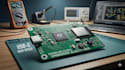
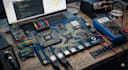
Need a reliable high speed PCB designer for your USB 3.2, USB-C, STM32, ESP32, or embedded electronics project? I design practical, manufacturing-ready high speed PCB solutions with careful routing, component selection, and signal integrity considerations.
WHAT I OFFER :
INTERFACES :
USB 3.2, USB 2.0, USB-C, UART, SPI, I2C, CAN, Ethernet, SDIO, I2S, WiFi and Bluetooth.
MCU SUPPORT :
STM32, ESP32, ESP32 S3, NXP and ARM microcontrollers.
SOFTWARE :
Altium Designer, KiCad, EasyEDA, LTspice, Proteus and STM32CubeIDE.
DELIVERABLES :
WHY CHOOSE ME :
Clean high speed PCB routing
Clear communication and practical support.
Contact me before ordering to discuss your USB speed, connector, PCB layer count, dimensions, impedance needs, and project and goals.
Can you design a USB 3.2 high speed PCB?
Yes. I can design USB 3.2 high speed PCBs for embedded devices, consumer electronics, development boards, & custom hardware. The design can include USB 3.2 Gen 1 or Gen 2, USB-C connectors, differential pair routing,impedance considerations, power delivery, protection,& suitable supporting component
Can you design USB-C PCB with USB 3.2 support?
Yes. I can design USB-C PCBs supporting USB 3.2 data communication, including USB-C connectors, high speed differential pairs, CC pins, power connections, protection circuits, ESD protection, and proper routing practices. Please provide your required USB speed, connector configuration and PCB size.
Can you handle high speed signal integrity and impedance controlled PCB layout?
Yes. I can create high speed PCB layouts with controlled differential pair routing, appropriate trace geometry, layer planning, return paths, and impedance requirements. I can also consider connector placement, via transitions, ground planes, and routing constraints to support reliable USB 3.2 high


