Browse categories
Explore
Fiverr Pro
English
$
USD
PCB Design Engineer PCB Layout Circuit Design
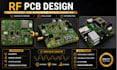
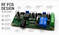
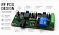
I'm an RF and PCB Engineer specializing in RF PCB, antenna, high speed, and high frequency wireless circuits. I build boards for wireless communication, GPS, WiFi, Bluetooth, and microwave applications, with controlled impedance routing for reliable signal performance.
What I offer:
Whether it's a simple wireless module or a complex microwave board, I make sure your layout meets signal performance standards and is ready for fabrication on the first try.
Message me your requirements before ordering so I can recommend the right package. Thanks!
Can you design RF PCBs for wireless and antenna applications?
Yes, I design RF PCBs for wireless communication, antenna integration, GPS, WiFi, and Bluetooth modules, with proper impedance-controlled routing for reliable signal performance.
What frequency range can you work with for high frequency PCB design?
I handle high frequency and microwave PCB designs from a few MHz up to several GHz, including RF front-end, filters, amplifiers, and transceiver layouts.
Do you provide impedance-controlled and controlled-impedance PCB routing?
Yes, every RF PCB includes impedance-controlled routing tailored to your board's stack-up and material (including Rogers or standard FR4), ensuring minimal signal loss.
Which software do you use for RF PCB and antenna design?
I use Altium Designer, KiCad, and EasyEDA for layout, with signal integrity and impedance calculations done using industry-standard methods for accurate RF performance.
Can you design multilayer or high speed PCBs with signal integrity in mind?
Yes, I design 2 to 12+ layer multilayer PCBs with signal integrity, EMI/EMC considerations, and controlled impedance for high speed and RF applications.
Do you deliver manufacturing-ready Gerber files and BOM?
Yes, every completed project includes DRC/ERC-checked Gerber files, drill files, and a Bill of Materials (BOM), so your board is ready to send straight to fabrication.


